
Pushing UberDDR3 Frequency Through RTL Cleanup - Post #18
- Angelo Jacobo
- Feb 13
- 8 min read

After a few years of working on UberDDR3, the design was in a good place feature-wise. ECC, dual-rank support, open-source tool flows, and ports to Lattice ECP5 were all working, and simulations were clean.
The one thing that kept bothering me was frequency, especially when using OpenXC7.

Over the past few months, I went back to the RTL with a more timing-focused mindset. I did not do a big redesign or add aggressive pipelining. Instead, I worked through the design one bottleneck at a time, separating combinational and sequential logic, registering decisions earlier, simplifying stall and control paths, and resizing logic where it clearly did not need to be that large.
In the end, those small iterations added up to more than a 40% increase in maximum frequency, without changing how the controller behaves.
This post walks through exactly what I changed, what worked, and how timing closure actually played out step by step.
Table of Contents
I. My Approach to Frequency Optimization
I did not start this with a fixed frequency target or a big plan in mind. Most of the time, I was just looking at whatever path was currently limiting the design from the nextpnr report, making one small change, and seeing what happened next.
One thing that became clear along the way is that frequency optimization is not linear. Fixing one path often just exposes another bottleneck, so frequency can go up and down between steps. When frequency dropped, it usually did not mean the change was wrong. In a few cases, it actually helped me see what was really limiting the design.
All of the results shown here uses the open-source synthesis and place and route toolchain from OpenXC7. From my experience, small RTL changes can sometimes lead to noticeably different results, so I focused less on individual numbers and more on the overall direction.
II. Baseline and Overall Progress
I started from a stable and fully functional version of UberDDR3 with the core features enabled, clean regression simulations, and passing formal checks. For reference, this is the exact GitHub commit of UberDDR3 which I used as the starting point.
All frequency numbers in this section come from the post place-and-route timing reports generated by the OpenXC7 open-source flow. For the actual implementation, I used one of the example_demo designs, targeting the ALINX Kintex-7 FPGA board.
With this setup, the baseline maximum frequency of the design was:
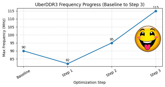
Baseline: 90 MHz
The table below shows how maximum frequency evolved as each change was applied. The intent here is not to show a smooth or ideal progression, but to reflect how timing closure actually played out as different bottlenecks were addressed.
Step | Modification | Max Frequency |
0 | Baseline | 90 MHz |
1 | Separate Combinational and Sequential Logic | 82 MHz |
2 | Register Conditions One-cycle Early | 95 MHz |
3 | Register Conditions in the FSM | 115 MHz |
4 | Rearrange Command Logic | 108 MHz |
5 | Flatten Stall Logic | 125 MHz |
6 | Resize registers and parameters | 132 MHz |
Here is a plot to show the progress of each step:

The next sections go straight into each step.
II.I Step 1: Separate Combinational and Sequential Logic
The first change I made was separating combinational logic from sequential logic more strictly. The two had grown mixed together over time, which made timing paths harder to see and reason about.
At that point, I found myself staring at timing reports and not being fully confident where certain decisions were actually happening. That was a good sign something needed cleanup.
Here is simple example of what I meant:
Before: combinational logic are mixed with sequential logic
After: combinational logic are in a separate always statement
This does not change functionality at all, but it makes intent much clearer. You can immediately see what feeds the register and what gets clocked. It also made the next step possible: once logic is structured like this, registering decisions earlier becomes much more straightforward.
For reference, here are the actual modifications I did for UberDDR3 for this step 1.
Frequency did not improve at this point, actually it got worse from 90 Mhz to 82 MHz!

Running PnR after this change was definitely not fun. I had not optimized anything yet, and suddenly the number dropped! If this is going to work, this is the moment where you trust the process and move on to the next change :)
II.II Step 2: Register Conditions One-cycle Early
The next thing that stood out was when decisions were being made. A lot of conditions used in nested logic are evaluated in the same cycle as the nested logic itself.
At first glance, it might seem like the fix is just to register those conditions. But doing that blindly would add an extra cycle of latency and potentially break the pipeline behavior. That was not what I wanted.
Instead, the idea here was to move the decision itself earlier, register it, and then let the existing nested logic use that registered decision one cycle later. The pipeline behavior stays the same, but the timing path is cut.
Here is simple example of what I meant:
Before: decision evaluated late and used inside deep nested logic
After: decision moved one cycle earlier and registered
This is also why Step 1 mattered. Once _q (sequential) and _d (combinational) logic were clearly separated, registering decisions early became straightforward: I could simply evaluate conditions using the _d signals, register them, and let the nested logic use the registered decision.
This did not change pipeline behavior, but it broke a long control path into two shorter ones. For reference, here are the actual modifications I did for UberDDR3 for this step 2.
Frequency finally improved here, from 82 MHz to 95 MHz, getting past the original 90 MHz baseline!

At this point I gained my confidence back; there are more steps remaining so let us see if we can maintain this momentum.
II.III Step 3: Register Conditions in the FSM
After Step 2, the calibration FSM stood out as the next timing hotspot. It had several conditions being evaluated deep inside state transitions, which made the control paths longer than they needed to be.
Unlike the previous step, this FSM is not pipelined, so I did not need to move decisions one cycle earlier. Simply registering the conditions was enough.
Here is simple example of what I meant:
Before: big condition checks live directly inside the FSM
After: decisions are registered first
For reference, here are the actual modifications I did for UberDDR3 for this step 3.
After fixing several of these cases, frequency jumped from 95 MHz to 115 MHz!
Let's roll! Onward to step 4!
II.IV Step 4: Rearrange Command Logic
After the big win in Step 3, I took a closer look at the stage-2 command logic. At the time, the flow was roughly:
read/write → activate → precharge
What bothered me was that some fairly large registers, like bank_active_row and bank_status, were only really relevant for precharge and activate, not for read or write. Yet because of the ordering, updates to those signals were still sitting behind the read/write decision logic.
So I tried flipping the order to:
precharge → activate → read/write
The idea was straightforward. If bank tracking is only modified during precharge or activate, then those cases should be handled first. That way, updates to bank_active_row and bank_status are not unnecessarily gated by the read/write path.
Here is simple example of what I meant:
Before: bank tracking logic is gated by read/write conditions
After: bank tracking logic is handled first and kept out of the read/write path
For reference, here are the actual modifications I did for UberDDR3 for this step 4.
Timing-wise, this step did not go as planned. Frequency dipped slightly, from 115 MHz to 108 MHz. That was a bit disappointing, but at this point I was mostly experimenting with structure and trying to see where the next bottleneck would move.

Hmmm let’s stay optimistic. Onward to Step 5!
II.V Step 5: Flatten Stall Logic
At this point, stage-2 was already correct functionally, but the stall logic around it had become more complicated than it needed to be. The same conditions were being checked in multiple branches, and stage2_stall was getting cleared in several different places.
Nothing was technically wrong, but from a timing point of view this meant stage2_stall sat at the end of a deep logic tree.
So the goal of this step was not to change behavior, but to flatten the logic.
Before: stage2_stall cleared in multiple places
After: one main decision, fewer layers
In the updated version, there is a single top-level assignment for stage2_stall, and only one place where it can be overridden. The conditions themselves did not change, but the structure did.
Another important detail is that the old logic relied directly on unregistered bank_status_d and bank_active_row_d. In the new version, those checks are effectively replaced by reusing already-computed and registered decision signals like stage2_do_act and stage2_do_wr_or_rd.
For reference, here are the actual modifications I did for UberDDR3 for this step 5.
Same meaning, cleaner timing. And this time, it paid off.
Frequency jumped to 125 MHz!

One last step to go!
II.VI Step 6: Resize Registers and Parameters
For the final step, I went after something simple but long overdue.
Over time, UberDDR3 accumulated a lot of generously sized counters, parameters, and registers. That made perfect sense early on. Bigger widths are safe, flexible, and future-proof. But once the design had settled and the behavior was well understood, some of those widths were just unnecessary weight for timing.
Before: oversized by default
After: sized to what’s actually needed
This pattern showed up in several places, especially delay counters and parameter-driven registers.
For reference, here are the actual modifications I did for UberDDR3 for this step 6.
Compared to the earlier steps, this one felt almost boring. No deep control changes, no pipeline tricks. Just careful cleanup, backed by regression and formal checks to make sure nothing broke when the widths are changed.
And of course, it paid off!
Maximum frequency: 132 MHz

III. Cross-FPGA Frequency Results
After finishing the RTL cleanup, I wanted to see how well the improvements translated across different FPGA boards, not just the one I was using during development.
For consistency, all results below use the same controller configuration, with basic features enabled and two-byte lanes used in all cases.
FPGA Board | Fmax (Before) | Fmax (After) | Increase |
Nexys Video (Artix-7) | 78 MHz | 120 MHz | 53% |
ALINX AX7325B (Kintex-7) | 90 MHz | 132 MHz | 46% |
QMTech Wukong (Artix-7) | 80 MHz | 116 MHz | 45% |
QMTech Kintex-7 | 100 MHz | 141 MHz | 41% |
Arty S7 (Spartan-7) | 83 MHz | 114 MHz | 37% |
Enclustra KX2-ST1 (Kintex-7) | 98 MHz | 131 MHz | 33% |
ALINX AX7103B (Artix-7) | 75 MHz | 98 MHz | 30% |
What stood out to me is that every board improved, even though the size of the gain wasn’t uniform. The increase ranged from about 30% to over 53%, depending on the device.
That variation is expected. Different FPGAs and speed grades respond differently to the same RTL. To me, this was a good confirmation that the work we did was not just about chasing one lucky timing report, but about making the RTL clearer and easier for the tools to optimize across different targets.
IV. Conclusion
This blog was not about finding a single trick to magically increase frequency. It was about taking a design that already worked, slowing down, and fixing one real bottleneck at a time.
Starting from a stable 90 MHz UberDDR3 design, I focused on cleaning up the RTL: separating combinational and sequential logic, registering decisions earlier, simplifying control paths, flattening stall logic, and finally trimming down registers that were bigger than they needed to be. None of these changes altered functionality, but together they made the design much easier to reason about and easier for the tools to optimize.
In the end, those small, deliberate changes pushed the maximum frequency, using OpenXC7 and fully open-source tools, with no aggressive pipelining and no architectural redesign.
That’s a result I’m genuinely happy with!
If there’s one takeaway here, it’s this: timing closure is often less about clever tricks and more about clarity. When the RTL becomes easier to understand, timing tends to follow.
Hopefully, this walkthrough gives you a few ideas to try on your own designs, especially if you’re working with open-source FPGA flows.
That wraps up this post. Catch you in the next blog post!


Comments